
Chip resistor laser trimming
Chip resistor trimming using lasers is a well proven and common technique used in the industry. This is especially so for passive trimming. Active trimming is useful too for final product characterisation and calibration of operation to global standards. However as products move rapidly in miniaturisation, there is need to squeeze the resistor size smaller and smaller with sizes like 03015. In this situation and to get higher resistance there is need to pack more trim lines in higher density thus approaching limits of laser spot size and trimming line width.
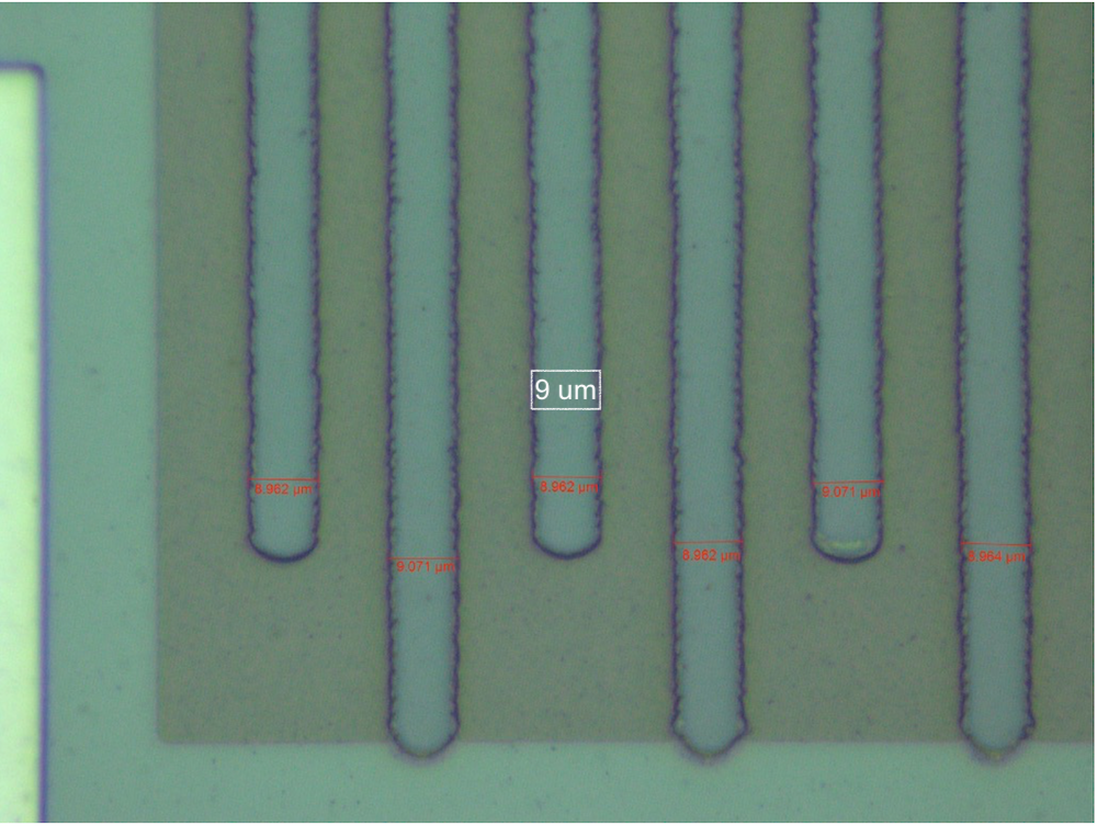
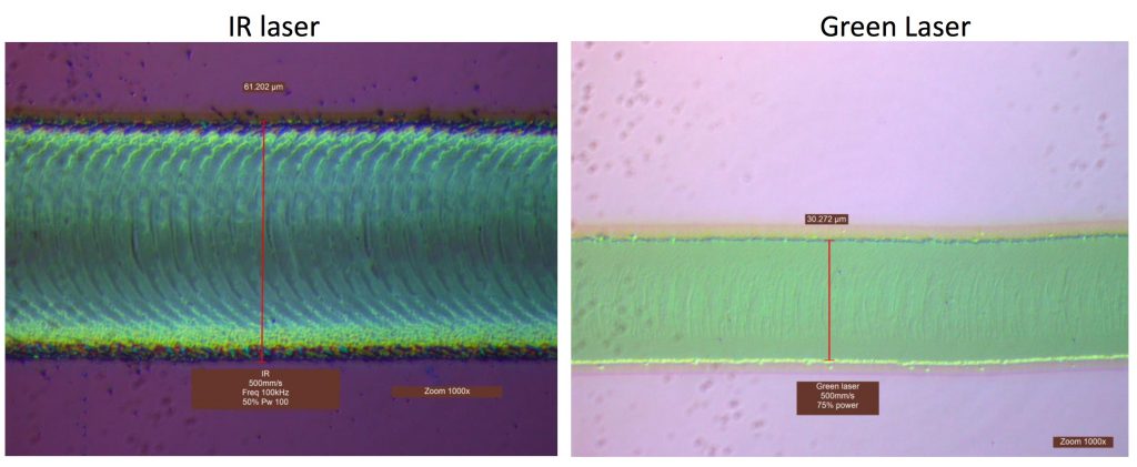
Trimming of resistor on ceramic with IR laser causes no damage to the ceramic base layer produces a clean cut with sophisticated optics and focusing techniques to achieve cut width of below 9 um. The cut is also clean with minimal particle generation.
Various trimming parameters were change in a series of experiments to characterise the process and to obtain best results.
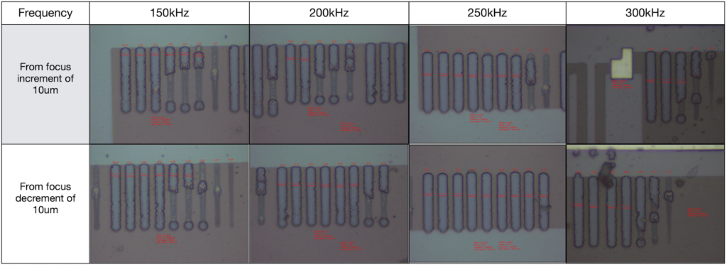
With Z step up down test, a higher frequency of 250 kHz will provide a wider Z tolerance range. The Z laser focus range was established to be +/- 50 um
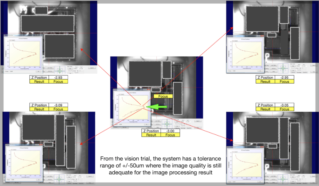
From the vision trial, the system was determined to have a tolerance range of +/- 50 um for image processing to be functional. Using our scanvision system we are able to find accurately the position of each resistor and land the laser to create precise trim cut lines in the midst of densely populated features.
Flat panel circuit traces thin film trimming
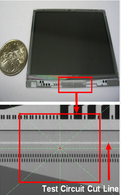
Test circuits are built into the LCD panels for the final test and after testing, the tracks of the test circuit have to be trimmed off. The accuracy requirement can be as high as +/- 10um.
ScanVision™ achieves high precision and speed by using the galvanometers movement to perform fiducial find, drift compensation, laser trim process and post trim check almost simultaneously whereby increasing the throughput by 3 fold over conventional systems.
Crystal tuning fork trimming
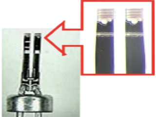
Quartz crystal such as those used in the watches can be trimmed with laser to achieve a specific resonance range. The accuracy requirement can be as high as +/- 15um.
The ScanVision™ with the fast galvanometers movements is able to identify the trim location and to perform the trim almost simultaneously with accuracy and doubling the throughput over the conventional system. Applicable to resistor and RFID antennae micro trimming etc.
Transparent ITO thin film on glass removal
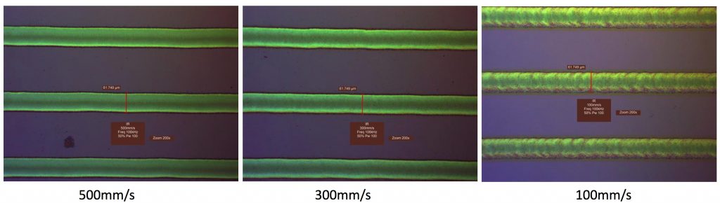
Cutting line width
The laser is able to provide good and clean isolation cuts on ITO as tested with electrical continuity probe test.
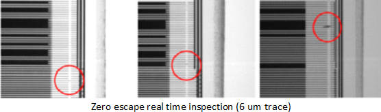
Hylax superior technology and expertise has enabled it to achieve trimming line width of 6 microns with pitch of 12 microns between lines. This is made possible with a combination of special optics, laser, electronics, scanhead and software innovation. With this achievement chip resistors can be used in even denser circuit boards and help produce smaller and smaller gadgets demanded by consumers nowadays.